|

Demonstration of Voltage Holding with Worlds-largest Fine Ceramic Ring
Progress on Development of 1 MV Accelerator for Heating and Current Drive in ITER
Mar. 17 , 2010
JAEA, Kyocera cooperation, and Hitachi Haramachi Electronics Co., Ltd. have succeeded in manufacturing of a large insulator for ITER neutral beam injector (NBI) composed of a worlds-largest fine ceramic ring. As a result of its high voltage test, the voltage holding capability of the insulator required in ITER NBI was verified for the first time in the world.
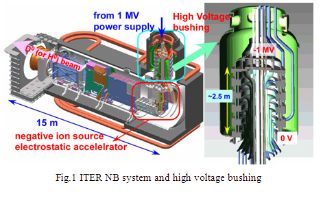
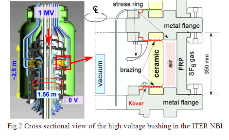
In the ITER NBI, a five-stage insulator (high voltage bushing) composed of large bore ceramic rings has been required to sustain 1 million volt (1 MV), as shown in Fig.1. Since many conductors penetrate inside the ceramic ring maintaining insulation of 1 MV, a dimension of the ceramic ring must be 1.56 m in diameter, 29 cm in height and 5 cm in thickness. However, the diameter has been limited less than 1 m in conventional manufacturing methods, and hence, the establishment of manufacturing method of the large ceramic ring has been a longstanding issue over ten years. The ceramic ring acts as a boundary between vacuum and gas region, and the ceramic ring must be joined with metal rings with high vacuum tightness, as shown in Fig.2. Typical technique to join ceramics and metal parts is brazing. Brazing on small ceramic is well-established technique, however, brazing of the large bore ceramic ring over 1 m had not been achieved. Then the establishment of joining technique of the large ceramic ring was another issue. In a verification of voltage holding capability of the insulator, suppression of breakdowns, which start from a joint of the ceramic and the metal due to a difference of their electrical properties, was a critical issue as well.
Toward the ITER NBI, JAEA has tackled the following technical development;
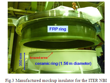
(1)With a newly-developed forming method, the worlds-largest ceramic ring (1.56 m in diameter) was successfully manufactured. This was performed under collaboration with Kyocera cooperation (Fig.3).
(2)In order to ensure the brazing process, JAEA developed equipments to equalize the adhesion metal distribution and thermal stress on ring-shaped joining surface. With those equipments, the large bore ceramic ring was successfully brazed with 3 mm thick Kovar rings. This was achieved as a collaborative work with Hitachi Haramachi Electronics Co., Ltd.
(3)Taking into account the breakdown triggered from the joint of the ceramic and metal, JAEA developed stress rings to suppress the breakdowns. The design of the stress ring was based on the knowledge and experience obtained through development of the accelerator for the ITER NBI.
In the high voltage test of the manufactured ceramic ring brazed with the Kovar ring as shown in Fig.3, 240 kilo volt was sustained stably over 1 hour. This is 20 % higher than a rated voltage for each ceramic ring (200 kilo volt), and the voltage holding capability required in the ITER NBI was verified for the first time.
The present result encourages the development of the ITER NBI. Spin-off effects in the industrial field such as the semiconductor manufacturing and the academic field such as the high energy physics are also expected.
|

Location of environment monitoring posts measuring amount of
radiation. (details)

International link directory of related websites.
|
